Advanced productive nanosystem
Up: productive nanosystems in general (including early precurser systems)
The focus here are productive nanosystems that are part of In-vacuum gem-gum technology and produce more of it.
For information about how to get to these systems please visit the main page about bootstrapping.
Productive nanosystems in general
This page here gives in depth details to the different aspects of advanced APM systems in general.
In the beginning of APM research only (molecular) assemblers where considered as a means for reaching the capability to produce macroscopic amounts of a product or block of material.
Here at the level of in-vacuum gem-gum technology it turns out that advanced nanofactories are more balanced and efficient than assembler systems.
At technology level I the border between minimal assemblers and rudimentary nanofactories is more blurred. A rudimentary nanofactory might be buildabel with exponential assembly instead of self replication but simplified two dimensional assembler linkages/mechanisms might work too.
On this wiki the term "productive nanosystem" is used as an umbrella term for both ideas.
Using the whole volume for the building process of the product rather than a layer in the "classic" nanofactory design could speed up the building process. But this will not be necessary for practical usage (wiki-TODO: find and link existing proof). If one builds a solid block product without voids/channels though one might end up being even slower than with the layer method due to the fractal growth speedup limit.
Assembly levels
The assembly process of AP products can be clearly divided in a number of subsequent steps no matter whether the concrete implementation of a productive nanosytem looks more like a nanofactory or more like an assembler system (assembler designs often skipped all assembly levels above I though). Those steps are implementation agnostic. Further details can be found on the assembly levels page.
Notes
- Depending on whether one assumes incremental improvement over technology levels or a more direct access there are two types of DME designs to choose from: pure hydrocarbon or various nonmetal including designs. Both have reason to be done.
- One may say that the concepts of nanofactories and assemblers are not sharply separable i.e. that they are merely the endpoints of a design continuum. To meet in the middle: The smallest possible grains of nanofactories (without the optional exponential assembly layers) somehow dispersed on a lattice in a volume could be looked at as a static configuration of quite big assemblers.
Assemblers
Note: The concept of assemblers is outdated!
Assemblers are Autogenous | mobile | productive | self replicating units.
That is after they replicated to a sufficiently large number they could start produce useful goods.
Assemblers are very hard to build directly and not an attractive aim point since they are very inefficient.
On a different note assemblers spawned the grey goo meme that latched on the overloaded and fuzzy term "nanotechnology" that sooner had become a major money source for non atomically precise research in the nanocosm. The result was a conflict leading to discredization cut of funding and censorship of everything related to APM. A development not in the interest of society.
An assembler could be thought of a very compact self contained (and probably in some way mobile) nanofactory with crippled exponential assembly and way too big mechanosynthesis cores.
Read more about assemblers on the molecular assembler main page.
Advanced nanofactories
- Main page: Gemstone metamaterial on chip factory
- Implementation details: Design of gem-gum on-chip factories
Two approaches to diamondoid nanofactories must be clearly discerned since the design objectives are very different.
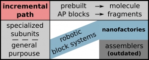
- Ones that are an attractive and sensible far term goal for the incremental technology path. e.g. the one sketched in Nanosystems.
- Ones that are designed to be easily buildable as easy as possible with a direct path approach. e.g. Chris phoenix nanofactory design skech
The attractive but distant aim point
How will a Nanofactory look like?
Lets start with the official productive nanosystem video - (high quality 94MB).
If this looks like a fantasy to you be aware that this is a desired aim point and certainly not the first thing one wants to build from scratch.
Also beside the sorting and atom deposition which are already quite concrete the further up steps serve more as a conception of what goes where rather than a construction plan.
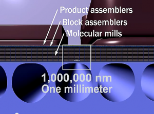
The blueish screen-shot on the right is from the video and shows all the assembly levels except IV. A strictly height ordered stratified layout is presented.
What is shown in the official productive nanosystems video:
Correspondence to assembly levels:
- Assembly level 0 and I are grouped together and represented by the "molecular mills" step.
- Assembly level II is represented by the "block assemblers" step.
- Assembly level III is represented by the "product assemblers" step.
- Assembly level IV is not integrated since its optional.omitted All assembly levels except IV
How much is conception only:
- In the "molecular mills" step The notion of "next stage" marks the point from 0a to 0b (filtering and tooltip preparation). It's quite concrete.
- The tooltip preparation process is depicted simplified (TODO: check in-how-far). For the actually more complex preparations cycles the tooltips (with tipcones) for mechanosynthesis can be merged with carriage structures that can be steered by rail switches.
- The shown reaction "which has been analyzed using advanced quantum chemistry techniques" is not RS6. (TODO: find out which it is supposed to be).
- Due to the assumption of limited to no steerability of the molecular mills a steerable routing system is needed for shuffling the produced DMEs in the right order. This routing system is conceptually shown between the "molecular mills" and the "block assemblers" step and in the video is called "transfer mechanism".
- Only mills are shown - a few more flexible but slower robotic manipulators doing mechanosynthesis are likely to augment them in a real system.
- The shown mill wheels could be extended to barrels. It is probably sensible to place more than just one atom per station. Some stripes of a whole layer maybe.
- The shown block and product assembler steps are rather wasteful of space and will probably look quite different in an actual design.
- Vacuum lock out is neither shown between "block" and "product assembler" step nor at the final macroscopic port. In a real system this must be integrated in at least one of these places.
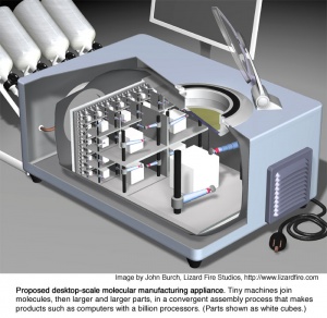
The artistic depiction of a nanofactory depicted in the grayish image on the right only shows assembly level IV (the optional higher convergent assembly stages). An iteration extruded 2D Fractal design is chosen.
Thorough analysis
For a detailed discussion of visit the page about advanced nanofactory design.
To find out how a nanofactory will look like more accurately one must start with the systems internal sub-product logistics (mechanosynthesis and assembly) since:
Nanosystems 14.4.1 "... the details of supporting systems ... are peripheral to the central issues of molecular manufacturing ... ... a reasonable estimate of overall system volume can be be had by summing the volumes of the assembly workspaces without describing a particulate three-dimensional layout. ..."* [[* Atom placement frequency
When subsystem sizes are roughly known one can start to contemplate about the possible spacial configurations by
making sure that production and consumption fits together at the borders between the assembly levels. This can be considered the level throughput balancing problem.
Its natural to think that it would be best to do mechanosynthesis in the whole nanofactories volume to get maximal productivity. That is to use dense construction style assembly without higher convergent assembly layers. Nanosystems ADDREF (known from early assembler system concepts). An estimation shows that running such a system at macroscopic speeds (which the DMME bearings can tolerate) leads to huge amounts of waste heat because of the high cumulative surface area of all the bearings. If one goes for maximum performance these levels of waste heat should be easily removable with AP pellet cooling systems. (other processing steps might limit assembly speed like e.g. molecule sorting Template:Todo: check) The problems are that the high mass throughput would create unacceptably high acceleration forces and the product couldn't be easily removed from the construction scaffold especially at those high speeds.
A more living-room friendly design can be reached by either going down with the operating speed or doing mechanosynthesis and basic assembly only in a thin layer extruding the products out. This is called manufacturing style assembly higher convergent assembly hierarchy can be put on top and the base layer could be broken apart and distributed in this hierarchy.
Designs for the direct path
There is an interesting article about Nanofactory design written by Chris Phoenix in 2003 "Design of a Primitive Nanofactory". More information can be founds on the "discussion of proposed nanofactory designs" page.
Link: The Nanofactory Collaboration.
General
Note that in a stratified design that uses convergent assembly that is strictly ordered after assembly levels a block made from eight blocks must come from only four ports of the stage below. Consequently the production frequency must double with every stage one goes down, which is no problem since objects of half size can move with twice the frequency (a scaling law). (In computer terms you extract an octree out of a a quadtree). The lowest levels (assembly levels <= II) are significantly slower then the simple mergement steps above.
Filling a whole volume with the basic assembly levels keeping macroscopic speeds would lead to ridiculously high mass throughput and heat generation. Slowing down to mediocre waste heat still leaves high productivity. Using a thin well coolable layer is the classical nanofactory approach.
Design levels
APM systems can depending on the size of the chunk of them that is under consideration be designed at three different levels:
- tooltip chemistry level
- atomistic mechanic level
- lower bulk limit
- system level
Further details can de found on the design levels page.
Diamondoid Molecular Elements (DMEs)
At the core an advanced productive APM systems consist out of DMEs.
DMEs can be designed either directly at the atomistic level or in lower bulk limit form.
One can classify DMEs into:
- Diamondoid Molecular machine elements DMMEs
- Diamondoid Molecular structural elements DMSEs
Furthere details can be found diamondoid molecular elements page.
Certain standard sets like housing components or a minimal set of compatible DMMEs are needed.
Potential structural and machine elements that seem suitable to port them to DME designs can be found here:
- Thingiverse collection I
- [Todo: add further resources]
Depending on the design different degrees of modifications need to be done.
All degrees of freedom need to be controlled, wall thicknesses need to be increased, atomic roughness must be considered, ...
Logistics
A lot of media need to be shoved around in a nanofactory.
Included are: data; energy; raw material; heat; waste; partly finished products; vacua (in some sense); noble gasses
The use of electricity is avoided at the lowest size levels since tunneling and conduction around bents are nontrivial.
See non mechanical technology path.
The routing of the structures bearing those different media i.e. the schematics to physical layout mapping is part of the system level design. Some structures bearing the transmitted media can be found on the "diamondoid molecular elements" page.
Data processing
Computation must be done reversibly since deleting data dissipated energy. More about this can be found on the "reversible data processing" page. For AP electronic computer technology go to: non mechanical technology path
For control a three layer hierarchical tree might suffice
- Top layer: external computer
- Intermediate layer: integrated nanoelectronics units
- Bottom layer: nanomechanic computation units (out of size reasons)
- Core: Semi Hard-cored conveyor belt systems (like molecular mills) & Manipulators (no active logic here)
Vacuum
Mechanosynthesis of diamondoid materials in t.level III needs to be done in a "perfect" vacuum (or noble gas). Actually this is the defining trait separating it from t.level II. Any free gas molecules would quickly react with the tooltips rendering them dysfunctional. From current perspective creation of "perfect" vacua seems illusionary. Any operator of an UHV system knows that it is impossible to get rid of all the gas molecules that are unavoidably adsorbed on the vacuum vessels walls. The current perspective is based on the current technology though. The vacuum vessels for APM systems of t.level III
- are cavities sized in the nanometer range - this increases the probability of having zero gas molecules captured inside
- have atomically precise maximally flat walls - not allowing for gas adsorption and allowing for maximally tight seals without out-gassing lubricants
- can utilize atomically tight positive displacement pumps for vacuum generation - no backflow
and are thus capable of creating sufficient vacua. (About sealings and pumps: Nanosystems 11.4.2 & 11.4.3)
For how to create and maintain vacuums with advanced AP systems see: Vacuum handling


